Posted on

New Product Release: ES620-C2 Inline TLP Test System for 100% Production Line Quality Control
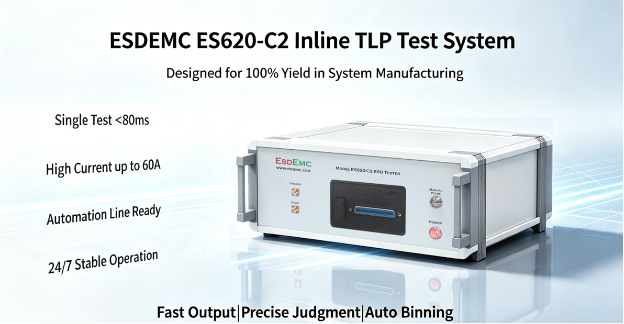
 ESDEMC Technology LLC is excited to announce the launch of the ES620-C2 Inline TLP Test System, our latest innovation designed specifically to bring laboratory-grade Transmission Line Pulse (TLP) IV testing directly to the semiconductor production line.

The Ripple Effect: Why System-Level Manufacturers Demand 100% Yield

The impact of a defective ESD protection device (such as a TVS diode) extends far beyond the component itself. For system-level manufacturers—from consumer electronics to automotive brands—using ESD devices with clamping voltages that deviate from their datasheet specifications can be catastrophic.

When an ESD event occurs, a compromised protection device fails to clamp the voltage safely, exposing expensive core SOCs and internal circuits to fatal damage. This not only severely impacts the overall system reliability but also drives up warranty, maintenance, and field repair costs exponentially. As a result, system-level manufacturers are increasingly mandating their component suppliers to guarantee a 100% tested outgoing yield to eliminate these hidden risks.

The Industry Bottleneck: Test Throughput

For component manufacturers, proving this 100% reliability is a challenge. The most critical performance metric—clamping voltage stability under high-current pulses—is best measured by TLP testing. However, traditional commercial TLP systems are designed for R&D. Extracting a complete I-V curve for a single device takes minutes, which is fundamentally incompatible with the high-speed throughput of modern production lines.

The Solution: ES620-C2

To bridge this critical gap, ESDEMC developed the ES620-C2 Inline TLP Test System. Engineered to integrate seamlessly with automated pipeline handling machines, the ES620-C2 transforms TLP from a slow qualitative R&D tool into a blazing-fast quantitative production gatekeeper.

Instead of sweeping a full curve, the ES620-C2 allows operators to preset a specific test voltage and defined Pass/Fail criteria. The system outputs the targeted TLP pulse, measures the voltage and current at the device under test (DUT), and determines if the clamping performance is acceptable—all in under 80 milliseconds per pulse.

By communicating the Pass/Fail judgment to the automated handler for real-time binning, the ES620-C2 allows component manufacturers to meet the strict 100% yield demands of system-level clients without sacrificing production efficiency.

Key Features of the ES620-C2:

  • Ultra-Fast Testing: Completes the entire pulse, measure, and judge cycle in < 80 ms per device.
  • High Output Capability: Delivers testing currents up to 60A.
  • Highly Configurable: Built-in hardware supports multiple selectable risetimes and pulse widths to meet diverse testing standards.
  • Automated Handler Integration: Perfect synchronization with production line machines for automatic Pass/Fail binning.
  • Production-Ready Reliability: Built for continuous, heavy-duty operation in manufacturing environments.

The ES620-C2 is now available to order. For more information, technical specifications, or to request a quote, please contact us.

Posted on

New Product Release: EPM-VF2 20 ps Rise Time TLP Pulse Module

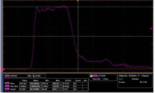
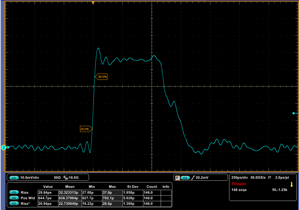
ESDEMC Technology LLC is excited to unveil the release of the stand-alone 20 ps Rise Time Pulse Module. The module delivers high-speed transmission line rectangular pulses with rise times of 30 ps (10–90%) and 20 ps (20–80%), enabling precise evaluation of advanced semiconductor devices. An example oscilloscope waveform measurement is shown below.

High-Speed Pulse Performance

The 20 ps rise time TLP pulse module has 50 Ω output impedance.  The default configuration provides a 500 ps pulse width, while other widths can be customized upon request to match specific test requirements. With its ultra-fast edge performance, the module is well-suited for Capacitively Coupled Transmission Line Pulse (CC-TLP) testing, as well as ESD sensitivity studies for high-frequency devices and circuits.

Flexible Integration with ES622

As an stand alone TLP pulse module, it integrates seamlessly with ESDEMC ES622 series TLP pulse generator, extending the platform’s capabilities for next-generation semiconductor research and reliability testing. The combination allows users to generate highly repeatable fast pulses for characterizing device behavior under realistic high-frequency stress conditions.

Applications

The 20 ps Rise Time Pulse Module addresses the needs of semiconductor engineers and researchers working on:

  • Wafer-level and package-level CC-TLP testing
  • ESD sensitivity testing of RF, high-speed, and advanced logic devices
  • Development of design guidelines and protection strategies for high-frequency circuits

By providing customizable pulse widths and ultra-fast rise times, the new module gives users greater flexibility in adapting their test environment to meet the evolving challenges of advanced semiconductor technologies.

ESDEMC Technology LLC,  a pioneering technology company, is committed to advancing the field of electronic components testing. With a focus on innovation, quality, and customer satisfaction, we continue to explore the future of semiconductor testing.

Posted on

ESDEMC Establishes European Service Center in Graz, Austria, in Collaboration with TU Graz to Strengthen Customer Support

March 1, 2025 – ESDEMC today announced the establishment of its European Service Center in Graz, Austria. This milestone reflects the company’s commitment to expanding its presence in the European market and to providing customers with more efficient pre-sales, after-sales, and technical support.

The new center will work closely with Professor David Pommerenke and his team at Graz University of Technology (TU Graz). A recognized authority in the field of electromagnetic compatibility (EMC), Dr. Pommerenke brings extensive expertise and academic insight. This collaboration will enhance ESDEMC’s ability to support European customers in EMC and ESD products purchasing and supporting, testing, design, and consulting services.

By setting up the European Service Center, ESDEMC aims to reduce response times and offer tailored solutions to help customers address increasingly complex EMC challenges. From automotive and aerospace to industrial automation and consumer electronics, ESDEMC’s specialized team and advanced test equipment will provide comprehensive support throughout the entire product cycle—from design to certification.

Europe has long been a strategic focus for ESDEMC. The Graz service center marks an important step in the company’s global development and demonstrates its ongoing commitment to European customers. Guided by the principles of customer focus and technical leadership, ESDEMC will continue to deliver high-quality ESD and EMC solutions that support both industry and academia in achieving sustainable growth under evolving regulatory standards.


Posted on

TR006 Die level CC-TLP Test Report

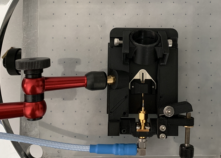
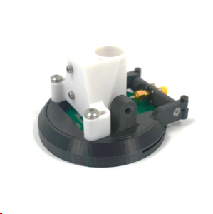
CC-TLP head CC-TLP-1

Download or View in PDF: TR006_ Die Level CC-TLP Test Report

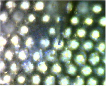
This report documents the CC-TLP (Charged Device Model – Transmission Line Pulse) testing performed on Die B at the die level. The purpose of this test is to evaluate the ESD (Electrostatic Discharge) robustness of the device under test (DUT) by applying CC-TLP pulses at various current levels and monitoring the leakage current before and after each pulse.


by Keith Miller, Joey Fang, Jared Floyd, Yingjie Gan

Posted on

Product Update: ES640 Introduces Wafer-Level JS002 CDM Testing Solution

January 18, 2025 – ESDEMC has introduced an update to the JS002 testing option for its ES640 system, adding a wafer-level version with a newly designed discharge probe. The enhancement enables CDM (Charged Device Model) testing on devices with pad sizes down to 50 μm, addressing the needs of advanced semiconductor manufacturing.

Since its release in 2020, the ES640 has supported user-replaceable 250 μm spring probes, Its spring-loaded design also helps reduce the risk of pad damage during testing. In 2023, a 120 μm option was introduced for specific customer needs.

The new wafer-level probe is produced with specialized materials and precision machining, allowing accurate contact on small pads while maintaining waveforms that comply with JS002 standards at 500 V. The new wafer-level probe further extends the flexibility of the system for semiconductor testing applications.


Posted on

ESDEMC and South China Normal University Establish Joint Laboratory

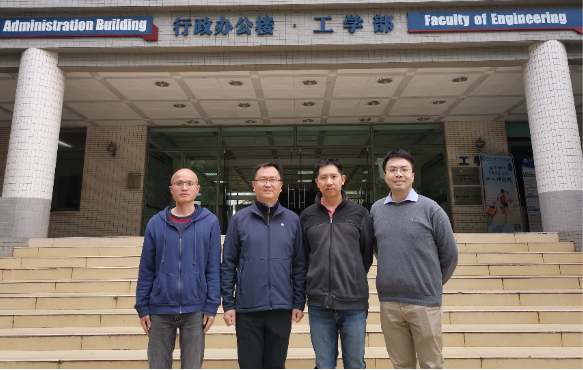
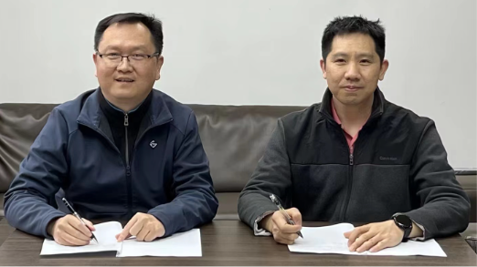
Recently, ESDEMC Technology LLC and the School of Engineering at South China Normal University signed a strategic cooperation agreement to establish a joint laboratory. The collaboration will focus on research in electrostatic discharge (ESD), electromagnetic compatibility (EMC), high voltage (HV), and radio frequency (RF) testing solutions. It aims to advance academic research and technological innovation in semiconductor field, with efforts in test methodology, standards development, and equipment design.

The partnership combines ESDEMC’s experience and strengths in developing, manufacturing, and supporting ESD/EMC test equipment with South China Normal University’s expertise in semiconductor materials, devices, and integrated circuits. Together, the two parties will conduct joint research on ESD/EMC testing technologies, standards, and equipment, while also fostering talent development to support technological progress and industrial growth.

This strategic cooperation represents a new step in linking industry and academia in semiconductor science. The joint laboratory is expected to provide both technological support and talent development to enhance the competitiveness of the semiconductor industry.


Posted on

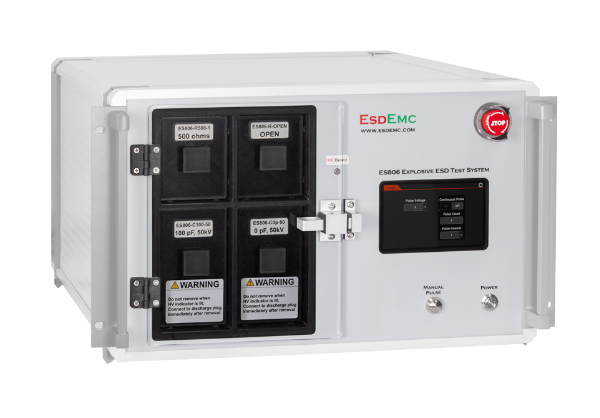
ESDEMC Introduces the New ES806 Explosive ESD Testing System

ESDEMC has announced the launch of the upgraded ES806 Explosive ESD Testing System. The new system features a refreshed design and significant improvements in usability, safety, and performance.

Redesigned Interface for Easier Operation

The ES806 now includes a large touchscreen interface, allowing users to conveniently set test voltage polarity, discharge levels, and discharge intervals. The updated design and improved user interaction make testing more efficient.

Pluggable RC Modules for Flexible Configuration

With its new pluggable RC module design, the ES806 allows users to easily switch modules according to testing requirements, supporting a wide range of scenarios. ESDEMC also offers customized RC modules to provide tailored testing solutions.

Enhanced Safety and Functionality

  • High-voltage safety detection: A safety check has been added to the RC module replacement area to ensure operator safety.
  • Emergency Stop: A dedicated emergency stop button allows immediate power cut-off in unexpected situations.
  • Continuous discharge: Adjustable continuous discharge capability supports more complex test requirements.

Safer Layout with Rear High-Voltage Output

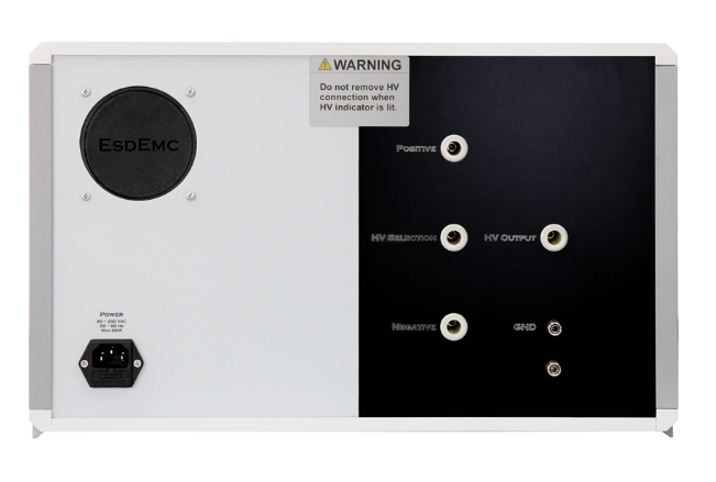
The high-voltage output interface has been relocated to the rear panel of the system, reducing operator exposure to high voltage and enhancing overall safety during testing.

Extended Voltage Range

The ES806 supports test voltages up to 50 kV, exceeding the 30 kV range common in similar systems, making it suitable for higher-standard testing requirements.

For more information about the ES806, please visit the ESDEMC product webpage: http://www.esdemc.cn/products/system-level-esd-test/es806-explosive-esd-test-system/


Posted on

TS020 Influence of 500R Resistor’s Bandwidth on HBM Calibration

TS020 Influence of Resistor Bandwidth on HBM Calibration featured image

Download Influence of 500R Resistor’s Bandwidth on HBM Calibration (PDF)

In the JS-001 standard, there is only one sentence describing the 500 Ohm evaluation load. However, the high-frequency characteristics of the resistor may vary significantly, and this variation can affect the verification of HBM current waveforms.

7 types of 500 Ohm resistors (R1 ~ R7) frequency responses were measured by VNA. HBM current waveform on these 500 Ohm resistors are captured and compared.

The result shows that even if the 500 Ohm resistor parameters meet the JS-001 requirements, same HBM tester’s current evaluation results may pass or fail the standard specifications with different resistors.

Posted on

ESDEMC Launches Upgraded CC-TLP-1 Probe for Wafer Level and Package Level CC-TLP Testing

ESDEMC announced the release of the upgraded CC-TLP-1 probe, featuring significant improvements in usability and performance for both wafer-level and package-level CC-TLP testing.

Enhanced Design for Easier Operation

The updated CC-TLP-1 probe system introduces:

  • Easy Bed Leveling – A redesigned leveling function that enables faster and more precise alignment between the ground plate and test sample, improving overall testing efficiency.
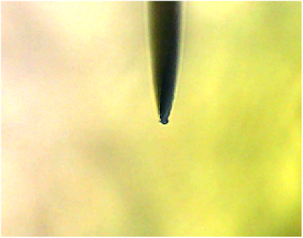
  • Easy Tip Replacement – Probe tips can now be replaced quickly, allowing users to switch between different tip sizes to meet a wide range of testing requirements.

High-Performance VF-TLP Generator and Accessories

When paired with the ESDEMC ES622 VF-TLP pulse generator, the CC-TLP-1 probe delivers:

  • 0.1 ns rise time
  • 1 ns pulse width

ESDEMC also offers customizable waveform parameters, enabling users to select rise times, pulse widths, and probe tip sizes to suit their specific applications.

Automated Test Software: Test Suite

The CC-TLP-1 works seamlessly with ESDEMC’s Test Suite software, providing an intuitive interface for test configuration, data acquisition, and result analysis. With support for automated test workflows, the software reduces complexity and enhances testing efficiency.

Applications

The CC-TLP-1 probe is designed for both wafer-level and package-level ESD testing and can be applied across semiconductors, integrated circuits, and automotive electronics. From R&D validation to production quality control, the CC-TLP-1 provides reliable data to support a wide range of testing needs.


Posted on

TS005 Characterization of TVS Diodes for ESD Protection Applications

Download Characterization of TVS Diodes for ESD Protection Applications (PDF)

TVS devices are designed to protect sensitive electronics from the damaging effects of electrostatic discharge (ESD). During normal operating conditions, TVS devices appear to be an open circuit (with small leakage current). Under stress conditions, these devices turn on, providing a low impedance path to the transient current. The voltage across the protected circuit is restricted to the clamp voltage of the TVS diode.

This technical slides introduced a typical methods to characterize TVS diodes:
1. VF-TLP characteristics:
(a) Transient waveforms; (b) IV curve & Turn on time; (c) Turn on voltage; (d) Dynamic resistance; (e) Clamping voltage; (f) Failure threshold
2. Effect on signal integrity
(a) Capacitance; (b) package inductance; (c) Insertion loss;
3. ESD generator contact mode behavior

Posted on

TS015 Introduction of Transmission Line Pulse (TLP) for ESD Analysis and Applications

Download Introduction of Transmission Line Pulse (TLP) for ESD Analysis and Applications (PDF)

TS015 Technical slides is the updated version of TS010. In this version, the TLP test procedures and applications are more detailed introduces.


Posted on

TS010 Introduction to RE Pre-Compliance Measurement with TEM Cell

Download Introduction to RE Pre-Compliance Measurement with TEM Cell (PDF)

Transverse-electromagnetic-mode (TEM) is an electromagnetic field pattern of radiation where both E and H fields are perpendicular to the direction of the radiation propagation.

A TEM Cell is an expanded coaxial transmission line (septum) that propagates TEM waves (within a cavity):
– E and H field are approximately uniform between the septum and cavity ceiling
– Approximately simulates a planar field in free space (377Ω far-field wave impedance)
– E field strength at the mid-point between the septum and cavity ceiling is related to the RF voltage between septum and cavity GND, and the septum to cavity ceiling height

The SAE J1752-3 standard defines a method for measuring EM radiation of an integrated circuit (IC) using a TEM Cell.
ESDEMC TEM Cell Products are specially designed to satisfy the requirements of the following standards:
▪ SAE J1752-3
▪ IEC 61967-8
▪ IEC 61967-2

Software solution is available for J1752-3 compliant RE testing and emissions level classification