ESDEMC Establishes European Service Center in Graz, Austria, in Collaboration with TU Graz to Strengthen Customer Support
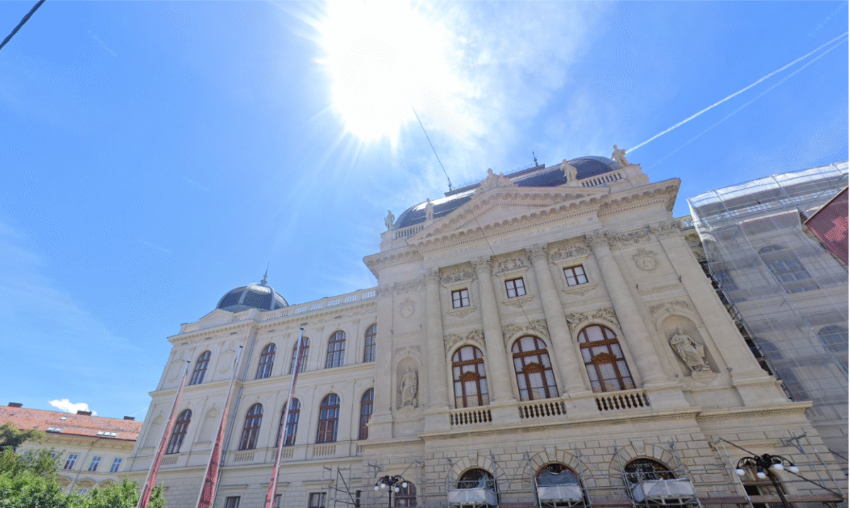
March 1, 2025 – ESDEMC today announced the establishment of its European Service Center in Graz, Austria. This milestone reflects the company’s commitment to expanding its presence in the European market and to providing customers with more efficient pre-sales, after-sales, and technical support.
The new center will work closely with Professor David Pommerenke and his team at Graz University of Technology (TU Graz). A recognized authority in the field of electromagnetic compatibility (EMC), Dr. Pommerenke brings extensive expertise and academic insight. This collaboration will enhance ESDEMC’s ability to support European customers in EMC and ESD products purchasing and supporting, testing, design, and consulting services.
By setting up the European Service Center, ESDEMC aims to reduce response times and offer tailored solutions to help customers address increasingly complex EMC challenges. From automotive and aerospace to industrial automation and consumer electronics, ESDEMC’s specialized team and advanced test equipment will provide comprehensive support throughout the entire product cycle—from design to certification.
Europe has long been a strategic focus for ESDEMC. The Graz service center marks an important step in the company’s global development and demonstrates its ongoing commitment to European customers. Guided by the principles of customer focus and technical leadership, ESDEMC will continue to deliver high-quality ESD and EMC solutions that support both industry and academia in achieving sustainable growth under evolving regulatory standards.